Photolithography, also known as optical lithography or UV lithography, is a microfabrication process used to pattern parts of a thin film or the bulk of a substrate. It plays a critical role in semiconductor manufacturing, MEMS fabrication, and printed circuit board (PCB) design. Photolithography enables the mass production of integrated circuits (ICs) and other micro-scale devices with extraordinary precision, down to the nanometer scale.
This article provides a detailed look into the principles, process steps, equipment, types, and applications of photolithography, as well as its limitations and future prospects.
1. What Is Photolithography?
Photolithography is a process used to transfer geometric patterns onto a substrate, typically silicon wafers, using light to selectively expose photoresist layers.
1.1 Definition
Photolithography is a microfabrication technique that uses ultraviolet (UV) light to transfer a geometric pattern from a photomask onto a photoresist layer, which is coated on a substrate.
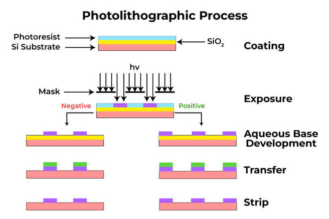
(geeksforgeeks)
1.2 Why Photolithography Matters
Photolithography is the backbone of semiconductor device fabrication, allowing for:
- Mass production of complex microstructures
- Precision patterning at nanometer resolution
- Layer-by-layer fabrication of integrated circuits
2. Key Components and Materials
2.1 Substrate
- Typically silicon wafers in microelectronics
- Can also be glass, metal, or polymer in MEMS or photonics
2.2 Photoresist
A light-sensitive material that undergoes chemical changes when exposed to UV light.
- Positive Photoresist: Becomes soluble where exposed
- Negative Photoresist: Becomes insoluble where exposed
2.3 Photomask
A plate containing the desired pattern, usually made of quartz with a chromium pattern.
2.4 Light Source
- Mercury-vapor lamps (i-line, h-line)
- Deep ultraviolet (DUV): 248 nm (KrF) or 193 nm (ArF)
- Extreme ultraviolet (EUV): 13.5 nm (advanced nodes)
3. Photolithography Process Steps
3.1 Surface Preparation
- Wafer cleaning using RCA or Piranha etch
- Dehydration baking to remove water
- Adhesion promoters like HMDS applied
3.2 Photoresist Application
- Spin coating spreads the resist uniformly across the wafer
- Typical thickness: 0.5–2 µm
3.3 Soft Bake (Prebake)
- Removes solvents to improve adhesion and uniformity
3.4 Mask Alignment and Exposure
- Align mask to wafer
- UV light passes through transparent areas of the mask, exposing the resist
3.5 Post-Exposure Bake (PEB)
- Optional step to improve resolution and resist contrast
3.6 Development
- Exposed photoresist areas are developed using a chemical developer
- Positive resist: exposed areas are removed
- Negative resist: unexposed areas are removed
3.7 Hard Bake
- Improves resist durability
- Reduces outgassing and enhances etch resistance
3.8 Etching or Deposition
- Transfer the resist pattern into the underlying layer using:
- Dry etching (e.g., reactive ion etching)
- Wet etching
- Material deposition
3.9 Resist Stripping (Resist Removal)
- Remove photoresist using plasma or chemical solvents
4. Types of Photolithography
| Type | Description | Resolution | Use Cases |
|---|---|---|---|
| Contact Printing | Mask touches resist surface | ~1 µm | MEMS, academic labs |
| Proximity Printing | Small gap between mask and wafer | ~2 µm | Early ICs, low-cost processes |
| Projection Printing | Lens projects pattern onto resist | ~10 nm (EUV) | Modern semiconductor fabrication |
| Stepper | Repeats small fields across wafer | 193 nm or 248 nm | Mass IC production |
| Scanner | Synchronizes mask and wafer movement | <10 nm (EUV) | 5 nm and smaller process nodes |
5. Photolithography Resolution and Challenges
5.1 Resolution Limitations
The resolution
is given by the Rayleigh criterion:
Where:
= wavelength of light
- NA = numerical aperture of the lens
= process-dependent factor
Lower wavelength and higher NA improve resolution.
5.2 Line Edge Roughness (LER)
Tiny deviations in pattern edges affect device performance.
5.3 Overlay Accuracy
Critical for aligning multiple layers in ICs.
6. Equipment Used in Photolithography
6.1 Spin Coater
Applies uniform resist layer on wafer
6.2 Mask Aligner / Stepper / Scanner
Aligns mask and wafer for exposure
6.3 Developer Track
Automates developing process
6.4 Baking Ovens (Hot Plates)
For soft and hard bakes
6.5 Etching Tools
Plasma etchers, wet benches
6.6 Metrology Tools
Measure pattern dimensions (CD SEM, ellipsometers)
7. Applications of Photolithography
| Industry | Application Example |
|---|---|
| Semiconductors | CPU, GPU, DRAM, NAND Flash |
| MEMS | Pressure sensors, accelerometers |
| Photonics | Waveguides, optical modulators |
| Biomedical Devices | Lab-on-chip devices, microfluidic channels |
| PCBs | Trace patterning in multilayer boards |
| Displays | Thin-film transistor arrays in LCDs and OLEDs |
8. Advancements in Photolithography
8.1 Deep Ultraviolet (DUV)
- Wavelengths of 248 nm (KrF) and 193 nm (ArF)
- Still widely used in semiconductor fabs
8.2 Immersion Lithography
- Uses water between lens and wafer
- Enhances NA and resolution (~45 nm nodes)
8.3 Extreme Ultraviolet Lithography (EUV)
- 13.5 nm wavelength
- Enables <7 nm node fabrication
- High cost, complex system (e.g., ASML EUV scanner)
8.4 Maskless Lithography
- Uses digital micromirror devices (DMDs)
- Suitable for prototyping or small-scale production
9. Limitations and Challenges
| Limitation | Description |
|---|---|
| Cost | EUV systems can exceed $150 million |
| Complexity | Multiple steps and tight tolerances |
| Defect Sensitivity | Particles, scratches on masks cause critical defects |
| Resolution vs Throughput | Trade-off between finer features and processing speed |
10. Alternatives to Photolithography
- Electron Beam Lithography (EBL): Higher resolution but slower
- Nanoimprint Lithography (NIL): Uses molds to imprint features
- Focused Ion Beam (FIB): Direct writing technique
- Laser Direct Writing (LDW): Maskless, used for prototyping
11. The Future of Photolithography
11.1 Sub-2 nm Fabrication
Pushing limits with EUV + multi-patterning
11.2 AI and Computational Lithography
Optimizing exposure patterns using machine learning
11.3 3D IC Stacking
Photolithography enables complex multi-layer integration
11.4 Sustainable Lithography
Developing eco-friendly resists, low-power UV sources, and chemical recycling
12. Summary Table: Key Takeaways
| Aspect | Photolithography Highlights |
|---|---|
| Core Principle | Light exposure through mask onto photoresist |
| Feature Sizes | Down to 5 nm (EUV) |
| Common Light Sources | i-line, DUV, EUV |
| Critical Equipment | Mask aligners, steppers, spin coaters, etchers |
| Major Applications | Semiconductor ICs, MEMS, PCBs, photonics |
| Major Challenges | Cost, resolution limits, process complexity |
13. FAQs About Photolithography
Q1: What is the main purpose of photolithography?
To pattern specific areas of a substrate to define circuit features and device structures.
Q2: What is the difference between positive and negative photoresists?
Positive resists become soluble upon exposure to light, while negative resists become insoluble.
Q3: What wavelengths are used in modern lithography?
- i-line: 365 nm
- DUV: 248 nm and 193 nm
- EUV: 13.5 nm
Q4: Why is EUV important?
It allows patterning at extremely small scales (sub-7 nm), essential for next-generation microprocessors.
Conclusion
Photolithography remains one of the most critical and sophisticated processes in modern microfabrication. From enabling the production of high-performance semiconductors to supporting MEMS and nano-scale devices, it is the engine of technological advancement in electronics, optics, and materials science.
As the industry pushes toward smaller nodes, higher performance, and greener solutions, photolithography is evolving with it—toward a future of even greater innovation.